


Altera FPGA MAX® 10
Les FPGA MAX® 10 d'Altera révolutionnent l'intégration non volatile en fournissant des capacités avancées de traitement dans un dispositif logique programmable à bas coût, à mise en marche immédiate et de petites dimensions. Avec un accès rapide à la documentation et au logiciel Quartus® II (BETA), les clients peuvent compiler et exécuter des analyses de temps pour une commercialisation accélérée. Les FPGA MAX 10 reposent sur la technologie flash intégrée 55 nm de TSMC, permettant une configuration avec mise en marche immédiate afin que les utilisateurs puissent contrôler rapidement la mise sous tension ou l'initialisation des autres composants dans le système. Les dispositifs comprennent également des capacités FPGA complètes telles que le traitement numérique du signal, la fonctionnalité analogique, la prise en charge du processeur intégré Nios II et des contrôleurs mémoire.
Instant-On, Embedded Dual Image Flash + Extra User Flash:
The MAX® 10 FPGAs include an integrated flash for self-configuring instant-on with dual image support to simplify the board design and save board space. Alternatively, can use the extra flash to store infrequent data logging or processor program code.
Single Power Supply Option:
The single-supply voltage operation makes this suitable for supervisory functions that need to be functional first before all the other system voltage rails have been enabled.
AI-capable DSP blocks:
These devices feature up to 144 embedded multiplier blocks, enabling performance/watt-efficient AI and edge computing solutions. Each block supports 18 x 18-bit or dual 9 x 9-bit multipliers, delivering the computational power needed for demanding AI tasks. These AI tasks include AI-assisted real-time signal processing, video analytics, and sensor fusion.
Integrated Dual Analog to Digital Converter:
The MAX 10 FPGAs consists of up to two built-in analog-to-digital converters with multichannel selection for monitoring power supplies or analog sensors.
Package Options:
The MAX 10 FPGAs contain a wide array of packages from tiny 3x3mm2 chip-scale packages to BGAs with 500 I/O and Quad-Flat Pack (QFP).
Caractéristiques
- Packaging:
- Low cost, small form factor packages - supports multiple packaging technologies and pin pitches
- Multiple device densities with compatible package footprints for seamless migration between different device densities
- RoHS6-compliant
- Core architecture:
- 4-input look-up table (LUT) and single register logic element (LE)
- LEs arranged in logic array block (LAB)
- Embedded RAM and user flash memory
- Clocks and PLLs
- Embedded multiplier blocks
- General purpose I/Os
- Internal memory blocks:
- M9K - 9Kb memory blocks
- Cascadable blocks to create RAM, dual port, and FIFO functions
- User flash memory (UFM):
- User accessible non-volatile storage
- High-speed operating frequency
- Large memory size
- High data retention
- Multiple interface option
- Embedded multiplier blocks:
- One 18×18 or two 9×9 multiplier modes
- Cascadable blocks enable the creation of filters, arithmetic functions, and image-processing pipelines
- ADC:
- 12-bit successive approximation register (SAR) type
- Up to 17x analog inputs
- Cumulative speed up to 1 million samples per second ( MSPS)
- Integrated temperature sensing capability
- Clock networks:
- Global clocks support
- High-speed frequency in clock network
- Built-in internal ring oscillator
- PLLs:
- Analog-based
- Low jitter
- High-precision clock synthesis
- Clock delay compensation
- Zero delay buffering
- Multiple output taps
- General-purpose I/Os (GPIOs):
- Multiple I/O standards support
- On-chip termination (OCT)
- Up to 720Mbps LVDS receiver and transmitter
- External memory interface (EMIF):
- Supports up to 600Mbps external memory interfaces
- DDR3, DDR3L, DDR2, LPDDR2 (on 10M16, 10M25, 10M40, and 10M50)
- SRAM (Hardware support only)
- For 600Mbps performance, –6 device speed grade is required
- Configuration:
- Internal configuration
- JTAG
- Advanced Encryption Standard (AES) 128-bit encryption and compression options
- Flash memory data retention of 20 years at +85°C
- Flexible power supply schemes:
- Single- and dual-supply device options
- Dynamically controlled input buffer power down
- Sleep mode for dynamic power reduction
Applications
- Industrial and automotive
- Drives, PV inverters, motor control, and sensor I/F
- I/O modules, surveillance, and machine vision
- Driver Assistance (ADAS), Electric Vehicle, ECU, and infotainment
- Wired/wireless communications
- I/O expansion and glue
- Chassis control
- Consumer
- Displays
- Portable, digital still cameras, and gaming
- Computer and storage
- Server board chassis control
- Multi-function printers
- Broadcast
- Military
Related Products

Altera Solutions d’alimentation Enpirion®
Dispositifs de gestion d’alimentation à haute fréquence et haut rendement pour FPGA, SoC, CPU, ASIC.

Altera FPGA optimisés en termes de puissance/prix
Familles de FPGA conçues pour l'optimisation en termes de prix/puissance et pour une haute intégration.
Development Tools

Altera Quartus® Prime Design Software
Multi-platform design environment for all phases of FPGA and CPLD design.
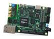
Altera MAX® 10 FPGA Evaluation Boards
General-purpose development platforms for applications like industrial and automotive.

Terasic Technologies DE10-Lite Board
A robust hardware design platform built around the Altera MAX 10 Field-Programmable Gate Array.
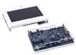
Terasic Technologies MAX 10 NEEK Evaluation Kit
A comprehensive design environment for Altera Max10 FPGAs with included LCD touch panel.

Alorium Technology Hinj Kit IoT & FPGA Development Solution
Features integrated connectivity with built-in driver support and programmable with Arduino.
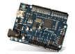
Alorium Technology XLR8 Development Board
Arduino-compatible board that can be used as a drop-in replacement for the Arduino Uno.

Altera Kit d'évaluation MAX® 10 DK-DEV-10M50F484-B FPGA
Fournit une plateforme d'utilisation facile pour évaluer la technologie MAX® 10 FPGA.

Altera Kit de développement FPGA MAX® 10 DK-DEV-10M50-C
Comprend une carte de développement MAX® 10, un adaptateur de secteur et un câble d'USB mini-B à USB.
Logic Elements
