


NXP Semiconductors LPC55S6x Arm® Cortex®-M33 Microcontrollers
NXP Semiconductors LPC55S6x Arm® Cortex®-M33 Microcontrollers (MCUs) feature dual Arm cores and Arm TrustZone® technology for industrial, building automation, Internet of Things (IoT) edge computing, diagnostic equipment, and consumer electronics applications. These devices feature advanced security features based on the Armv8-M architecture with a low-power 40nm embedded flash process.
The LPC55S6x Microcontrollers provide a unique set of security blocks, providing layers of protection for embedded systems while protecting end products from unknown or unexpected threats over its life cycle. These blocks include SRAM PUF for a based root of trust and provisioning, real-time execution from encrypted images, Arm TrustZone technology for system-wide hardware isolation for trusted software, and debug authentication capabilities.
The NXP LPC55S6x Microcontrollers feature an integrated power management unit to lower power consumption and achieve up to 32µA/MHz efficiency at the 96MHz core clock frequency. The devices boast a dedicated DSP hardware accelerator leveraging the co-processor extensions available in the Armv8-M architecture and extending the processing capability of the CPU while maintaining full ecosystem and toolchain compatibility. The microcontrollers offer enhanced real-time parallelism, using an autonomous programmable logic unit (PLU) for offloading and execution of user-defined tasks.
The LPC55S6x Microcontrollers are offered in HLQFP-100, VFBGA-98, and HTQFP-64 packages, with a -40°C to +105°C operating temperature range.
Features
- Arm Cortex-M33 Core
- Arm Cortex-M33 processor, running at a frequency of up to 150MHz
- TrustZone, Floating Point Unit (FPU) and Memory Protection Unit (MPU)
- Arm Cortex-M33 built-in Nested Vectored Interrupt Controller (NVIC)
- Non-maskable Interrupt (NMI) input with a selection of sources
- Co-processor
- Arm Cortex-M33 co-processor
- Running at a frequency of up to 100MHz
- The configuration of this instance does not include MPU, FPU, DSP, ETM, and TrustZone
- System tick timer
- CASPER Crypto co-processor to enable hardware acceleration for certain asymmetric cryptographic algorithms
- PowerQuad hardware accelerator for (fixed and floating point) DSP functions
- Arm Cortex-M33 co-processor
- On-chip Memory
- Up to 640KB on-chip flash program memory with a flash accelerator and 256-byte page erase and write
- Up to 320KB total SRAM consisting of 288KB on the system bus and 32KB on Core Bus
- Security Features
- Arm TrustZone enabled
- PRINCE module for real-time encryption of data being written to on-chip flash and decryption of encrypted flash data during reading to allow asset protection
- AES-256 encryption/decryption engine
- Secure Hash Algorithm (SHA2) module supporting secure boot with dedicated DMA controller
- Physical Unclonable Function(PUF) using dedicated SRAM for silicon fingerprint. PUF can generate, store, and reconstruct key sizes from 64 to 4096 bits. Includes hardware for key extraction
- Random Number Generator (RNG)
- 128-bit unique device serial number for identification (UUID)
- Secure GPIO
- Serial Interfaces
- Flexcomm Interface contains up to nine serial peripherals. Each Flexcomm Interface can be selected by software to be a USART, SPI, I2C, and I2S interface
- I2C-bus interfaces support Fast-mode and Fast-mode Plus with data rates of up to 1Mbit/s and with multiple address recognition and monitor mode
- USB 2.0 full speed host/device controller with on-chip PHY and dedicated DMA controller supporting crystal-less operation in device mode
- USB 2.0 high-speed host/device controller with on-chip high-speed PHY
- Digital Peripherals
- DMA0 controller with 23 channels and up to 22 programmable triggers, able to access all memories and DMA-capable peripherals.
- DMA1 controller with 10 channels and up to 16 programmable triggers, able to access all memories and DMA-capable peripherals
- Secured digital input/output (SD/MMC and SDIO) card interface with DMA support. SDIO with support for up to two cards. Supported card types are MMC, SDIO, and CE-ATA. Supports SD2.0, and SR25
- CRC engine block can calculate a CRC on supplied data using one of three standard polynomials with DMA support.
- Up to 64 General-Purpose Input/Output (GPIO) pins.
- GPIO registers are located on the AHB for fast access. The DMA supports GPIO ports.
- Up to eight GPIOs can be selected as Pin Interrupts (PINT), triggered by rising, falling, or both input edges.
- Two GPIO Grouped Interrupts (GINT) enable an interrupt based on a logical (AND/OR) combination of input states.
- I/O pin configuration with support for up to 16 function options.
- Programmable Logic Unit (PLU) to create small combinational and/or sequential logic networks, including state machines
- Analog Peripherals
- 16-bit ADC with five differential channel pair (or 10 singled-ended channels), and with multiple internal and external trigger inputs and sample rates of up to 1.0MSamples/sec. The ADC supports two independent conversion sequences
- Integrated temperature sensor connected to the ADC
- Comparator with five input pins and external or internal reference voltage
- Timers
- Five 32-bit standard general-purpose asynchronous timers/counters, which support up to four capture inputs and four compare outputs. Specific timer events can be selected to generate DMA requests
- One SCTimer/PWM with eight input and ten output functions (including capture and match). Inputs and outputs can be routed to or from external pins and internally to or from selected peripherals. Internally, the SCTimer/PWM supports 16 match/captures, 16 events, and 32 states
- 32-bit Real-time clock (RTC) with 1s resolution running in the always-on power domain. A timer in the RTC can be used for wake-up from all low power modes, including deep power-down, with 1ms resolution
- Multiple-channel multi-rate 24-bit timer (MRT) for repetitive interrupt generation at up to four programmable, fixed rates
- Windowed Watchdog Timer (WWDT) with FRO 1 MHZ as a clock source
- Micro-Tick Timer running from the watchdog oscillator can be sued to wake-up the device from sleep and deep-sleep modes
- 42-bit free running OS Timer as continuous time-base for the system, available in any reduced power modes.
- Clock Generation
- Internal Free Running Oscillator (FRO). This oscillator provides a selectable 96MHz output, and a 12MHz output (divided down from the selected higher frequency) that can be used as a system clock. The FRO is trimmed to +/- 1% accuracy over the entire voltage and temperature range
- 32kHz Internal Free Running Oscillator FRO. The FRO is trimmed to ±1% accuracy over the entire voltage and temperature range
- Internal low-power oscillator (FRO 1MHz)
- Crystal oscillator with an operating frequency of 1MHz to 25MHz. Option for external clock input (bypass mode) for clock frequencies of up to 25MHz
- Crystal oscillator with 32.768kHz operating frequency
- PLL0 and LLL1 allow CPU operation up to the maximum CPU rate without the need for a high-frequency external clock
- Clock output function with a divider to monitor internal clocks
- Frequency measurement unit for measuring the frequency of any on-chip or off-chip clock signal
- Power Saving Modes
- Integrated Power Management Unit (PMU) to minimize power consumption
- Reduced power modes: Sleep, deep-sleep with RAM retention, power-down with RAM retention and CPU0 retention, and deep power-down
- Configurable wake-up options from peripheral interrupts
- The Micro-Tick Timer running from the watchdog oscillator, and the Real-Time Clock (RTC) running from the 32.678kHz clock, can be used to wake-up the device from sleep and deep-sleep modes
- Power-On Reset (POR)
- Brown-Out-Detect (BOD) with separate thresholds for interrupt and forced reset
- Additional Information
- Operating from an internal DC-DC converter
- Single power supply 1.8V to 3.6V
- JTAG boundary scan supported
- Operating temperature range -40°C to +105°C
- Available in HLQFP-100, VFBGA-98, and HTQFP-64 packages
Applications
- Consumer electronics
- Diagnostic equipment
- Building control and automation
- Secure applications
- Industrial IoT
- Machine learning
Block Diagram

Related Products
NXP Semiconductors pour l'IdO- autonomiser la périphérie partout
Un vaste portefeuille pour servir les marchés cibles critiques de l'IdO.

NXP Semiconductors Microcontrôleurs ARM® Cortex®-M33 série LPC5500
Microcontrôleurs ARM Cortex-M33 offrant un niveau de performances et de sécurité avancé avec un cœur à bon rendement énergétique.
NXP Semiconductors Microcontrôleurs LPC550x/S0x
Offre une sécurité avancée, ce qui la rend idéale pour les applications industrielles, IdO et générales embarquées.
Supporting Software

NXP Semiconductors Expérience du développeur MCUXpresso
Optimise, facilite et aide à accélérer le développement de systèmes embarqués d’applications.
Development Tools
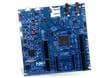
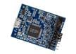
NXP Semiconductors LPCXpresso55S69 Development Board (LPC55S69-EVK)
Evaluates LPC55S6x MCU and features an onboard debug probe, audio subsystem, and accelerometer.
NXP Semiconductors Sonde de débogage MCU - Link Pro SWD
Outil de débogage à faible coût et riche en fonctionnalités pour les microcontrôleurs basés sur Arm® Cortex®-M.
NXP Semiconductors Sonde de débogage de liaison avec les MCU
Carte puissante utilisable avec l’IDE MCUXpresso et compatible avec des IDE tiers.